PM Modi to inaugurate Semicon India 2026: A look at India’s renewed semiconductor focus
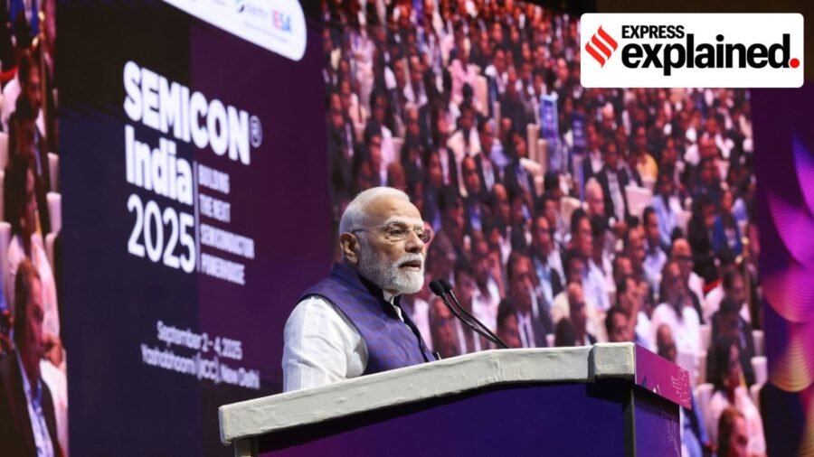
Prime Minister Narendra Modi will inaugurate the fifth edition of Semicon India 2026 on Thursday (September 17), as New Delhi looks to attract global chip manufacturing companies and talent, and showcase its fledgling semiconductor base that did not exist just half a decade ago.
The three-day conference and exhibition, being held from September 17 to 19, will be organised on the theme ‘Silicon to Systems: Building the Ecosystem’. It will bring together global and Indian companies, policymakers, investors, researchers, start-ups, and academic institutions from across the semiconductor and electronics value chain.
The conference will focus on advancing collaboration, investment, innovation and talent development in India. Parallel sessions will cover advancements in the display industry, six Country Roundtables designed to facilitate collaboration and joint ventures, a forum on women’s leadership, among other sessions.
Story continues below.
Subscribe to see fewer ads.
On Wednesday (September 16), the PM chaired a roundtable with heads of leading chip companies, such as Micron Technology, ASML, Infineon Technologies, Applied Materials, Tokyo Electron AMD, Intel, and Tata Electronics, among others.
During the meeting, the PM emphasised the importance of close collaboration between the Government and the semiconductor industry, and highlighted India’s strong foundation of talent, technology adoption and infrastructure, calling for greater industry participation in skilling, innovation and emerging technologies, according to a statement by the PM’s office.
India’s chip push: key focus on domestic design capabilities
The conference comes two months after the Centre announced the second iteration of its Semiconductor Mission, with an outlay of Rs 1.27 lakh crore, and a particular focus on incentivising domestic chip design, and localising the broader supply chain of ancillary industries, such as equipment manufacturers, and producers of specialty gases and chemicals. Under the first leg of the scheme, India managed to attract 12 chip manufacturing and assembly projects, including a fabrication facility being set up by the Tata Group.
Story continues below this ad
Semiconductor design and production are critical to building tech products such as laptops, phones and AI models today, and this design push seeks to address a key gap in India’s semiconductor ambitions.
Semicon 2.0 seeks to build more Indian-owned intellectual property and fabless semiconductor companies — firms that design and sell chips while outsourcing the work of physical fabrication.
The scheme targets semiconductor technologies considered important for national security and critical infrastructure. The government will identify IP, chips, systems-on-chip (SoCs) and modules that it wants developed, including building blocks for compute, memory, radio frequency, power, networking and sensors.
It also focuses on commercial chip-design companies, where the government will provide access to expensive electronic design automation tools, multi-project wafer fabrication services and other systems to eligible companies.
Story continues below this ad
For this commercial category, eligibility has also been widened to companies owned and controlled by Overseas Citizens of India (OCIs), provided they are incorporated and headquartered in India and maintain a significant operational and manpower presence here. The IP and associated design and development files must remain in India.
Broader ecosystem play
The scheme is also aimed at filling gaps across the semiconductor supply chain.
Companies setting up semiconductor-equipment R&D facilities, plants manufacturing wafers, photomasks, photoresists, substrates, chemicals and gases, testing facilities, or units producing semiconductor equipment and components can receive 30% capital expenditure support. Equipment manufacturers will additionally get a production-linked incentive that declines from 10% to 2% over five years on the value of their bill of materials sourced domestically.
Large silicon wafer fabs will be eligible for 40% capex support, while compound semiconductor, photonics, sensor and discrete semiconductor fabs can receive 35%. Advanced chip-packaging facilities will receive 35%, compared with 25% for legacy packaging. These incentives have reduced compared to the uniform 50% capex subsidy the government had offered in the first iteration of the scheme, introduced in 2021 to build a full-stack chip ecosystem.
Talent development
Story continues below this ad
Talent development has been carved out as a separate pillar under Semicon 2.0. The government wants to train not only chip designers, but also engineers, researchers, technicians and shop-floor operators required across fabrication and packaging plants.
“India achieved its target of developing 85,000 semiconductor engineers over a period of 10 years in just four years, and has now set a new target of developing one lakh more engineers… Students from tier-II and tier-III cities have already designed more than 250 chips… The semiconductor ecosystem being developed in India is also expected to create 50,000 – 60,000 direct jobs,” IT Minister Ashwini Vaishnaw had earlier said.
On the design side, support will cover access to advanced chip-design tools, multi-project wafer services and post-silicon validation facilities. On the manufacturing side, the scheme will support dedicated training infrastructure and strengthen existing nanofabrication and process laboratories. Eligible projects can receive support of up to 75% of their cost, including state incentives.

Graphs, Data, Perspectives | Why the US Fed hiked rates, and what to make of its decision
By Sohail Khan · 17 Sep
‘Is it normal to have a blood sugar level of 110 at age 54, or am I diabetic?’
By Sohail Khan · 17 Sep
Why are moths attracted to bright lights?
By Sohail Khan · 17 Sep
Leave a Reply